Chapter II - Optically Transparent electrode (Part 1)
1. Requirements for optically transparent electrodes
The optically transparent electrode used in spectroelectrochemistry should meet the requirements of both spectral and electrical properties. The ideal optically transparen electrode should have good light transmission and low resistance value. In fact there are not many materials that meet these two requirements, and a compromise approach is generally used 2-1).
Several types of optically transparent electrodes are discussed below.
2. SnO2 and In2O3 optically transparent electrode
2.1 SnO2 optically transparent electrode
SnO2 glass coated with a thin layer of Sb doped with its trade name is Nesa glass. The coating is usually about 0.8 to 1.0 µm. It is made by spraying an acidic solution of SnCl4 onto a glass or quartz substrate and thermally decomposing it. The pure tin oxide film has polycrystalline characteristics, and its conductivity is due to the oxygen defect and the defect structure of interstitial tin atoms, and the doping of oxygen impurities in the cassiterite crystal. Doped tin oxide is more commonly made by adding antimony atoms. As the core of Sn(IV) in the tin oxide lattice is replaced by antimony Sb(III), the density of n-type carriers increases by more than 1020 carrier⁄cm2 can reach a surface resistance of less than 15 Ω⁄sq. These SnO2 films can serve as a completely inert and chemically stable surface in electrochemical research.
The typical spectrum of n-type tin oxide SnO2 coating on the transparent substrate is shown in Fig. 2-1. At 360 nm on the glass substrate, the sharp attenuation of the light transmittance is due to the absorption of the glass itself. Coated on a quartz plate, the outside direction of the optical window can be extended to the wavelength of 300nm. Therefore, the SnO2 optically transparent electrode is only suitable for research in the visible light range.
Fig. 2-1. Transmission spectra of Sn02 coating on different substrates.
(a) Glass, 3 Ω⁄sq; (b)Vicor, 6 Ω⁄sq; (c) Quartz,12 Ω⁄sq2-1)
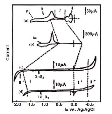
Fig. 2-2. Comparison of current-potential curves of Pt, Au, SnO2 and In2O3 in 1M H2SO4 solution.
The range of potentials applied to the SnO2 coated electrode in aqueous solution is much wider than that applied to the Pt and Au electrodes 2-2). Figure 2-2 is a comparison of the current-potential curves for Pt, Au, SnO2 and In2O3 in a 1 M H2SO4 medium. The current-voltage (i-E) curves can be divided into three main regions, which have been studied extensively for both platinum and gold electrodes. For both electrodes, if the potential is maintained in the hydrogen emitting region for a period of time, the metal film will be irreversibly damaged.
For tin oxide and indium oxide, the charge on the electrode changes monotonously in the entire area. Because the electrode is already an oxide, it is usually the highest oxidation state of the metal. When the potential increases in the positive direction, there is no oxide formation. Obviously, the potential of Faraday current region 1 is as wide as 1.5 V. The boundary of these oxide films in the direction of positive potential zone III′ is for the precipitation of oxygen, and the boundary zone II′ in the direction of negative potential is the oxide reduction to metal The lower valence state of the oxide, hydrogen evolution or surface reduction to the metal state zone II″, so similar to the metal electrode. Therefore, delay electrolysis at a very negative potential will produce irreversible and harmful changes.
It can be seen from Fig. 2-2. that compared with platinum or gold electrodes, SnO2 and In2O3 tin oxide and indium oxide electrodes have a wider redox potential window, however, carriers will be generated at a potential that is more positive than the potential window. Therefore, the rate of any Faraday transfer (such as oxidation of trivalent cerium) under a very positive potential is limited by the charge transfer process of the semiconductor film. In the case of low doping content, the tunneling effect may be the main electron transfer mechanism. In the case of high doping content, other factors including the composition of the surface oxide may be the main factor affecting electron transfer.
The hydrogen evolution zone II on the metal film electrode is replaced by II′, II″ on the semiconductor. The difference between the zone I and II′ is that the small Faraday current may be related to the surface electrode reaction, and its current size is the same as that of the zinc oxide electrode surface Part of the reduction is related to the current, which is only observed in deoxygenated solutions (less than 10 - 5 mol⁄L O2 and increases in alkaline solutions. The potential passes through the region II&pirme; to produce irreversible reduction of semiconductors. Due to some surface degradation such as the dissolution of the layer, zinc oxide coated electrodes are not suitable for research in high alkaline pH solutions. Indium oxide motors behave similarly to tin oxide.
In addition, the polyester sheet coated with metal oxide can also be used as a optically transparent electrode, showing a lower impedance (10 -200 Ω), and it is much cheaper than quartz and glass as a substrate. The flexibility of the sheet makes it suitable for non-planar geometries, and the electrode is relatively stable in water and non-aqueous solvents. Its main disadvantage is still limited due to the absorption of the polyester plastic substrate in the infrared and ultraviolet regions. For applications in the visible light range.
2. 2 In2O3 optically transparent electrode
In2O3 crystal has two crystal types, cubic phase (wurstite type) and triangular phase (corundum type). Theoretically, pure indium oxide film has high resistance and almost no conductivity, but its performance can be effectively adjusted by doping. Doping Sn, Mo, Sb and other elements can obtain N-type indium oxide film materials with ideal electrical properties , Significantly improve the conductivity of the indium oxide film and improve the conductivity of the film. At present, the most studied and most excellent comprehensive performance is mainly tin-doped indium oxide film, namely ITO film (Indium Tin Oxide). Tin-doped indium oxide (ITO) films are widely used as transparent electrodes in optoelectronic devices. Including liquid crystal displays, plasma display panels and solar cells. Although the ITO film shows transparency and conductivity at high room temperature, the latter is severely damaged at high temperature. In practice, when the ITO film is exposed to high temperatures above 300°C, its electrical properties will be affected. The resistance has increased by more than three times.
Indium tin oxide (ITO) films are widely used as transparent electrodes in optoelectronic devices. Including liquid crystal displays, plasma display panels and solar cells. Although the ITO film shows transparency and conductivity at high room temperature, the latter is severely damaged at high temperature. In practice, when the ITO film is exposed to high temperatures above 300 °C, its electrical properties will be affected. The resistance has increased by more than three times.
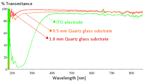
Fig. 2-3. The light transmittance of the ITO electrode on the quartz substrate is compared with the 0.5 mm and 1 mm quartz substrate.
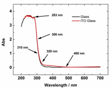
Fig. 2-4. Comparison of the absorption spectra of the ITO electrode on the glass substrate and the glass substrate.
Fig. 2-3. shows the light transmittance comparison between the ITO electrode on the quartz substrate and the 0.5 mm, 1 mm quartz substrate. The light transmittance of the quartz substrate decreases slightly as its thickness increases. It can be seen that the ITO on the quartz substrate transmits light in the visible light range, and light in the ultraviolet range cannot pass. It is difficult to measure the absorption spectrum in the ultraviolet region.
Figure 2-4 shows the comparison of the absorption spectra of the ITO electrode on the glass substrate and the glass substrate. It can be seen that for the ITO electrode, there is no obvious difference between the absorption spectrum shape of the quartz substrate and the glass substrate.
3. Pt and Au Thin film transparent electrode
The main disadvantages of the above-mentioned metal oxide electrodes are the poor reproducibility and high resistance of the electrodes, and they are only suitable for research in the visible light range. They are later replaced by vacuum sprayed Pt and Au thin films (<5000 angstroms), which can be properly prepared. These films have good mechanical stability, low resistance and reasonable light transmittance.
The film manufacturing steps are as follows.
- Strictly clean the transparent substrate surface (glass or quartz), and then ion bombard the substrate surface under vacuum to ensure good adhesion of the metal film on the substrate.
- On the substrate coated with Bi and Pb in advance, gold is deposited in a high vacuum, and the thickness of the film is controlled by controlling the deposition time.
- Control temperature annealing to change the conductivity and light transmittance of the film.
The deposition of Pt film is similar to this, the difference is that Pt can be sprayed directly on the substrate. The Pt film is mechanically stable. When the film is oxidized or polarized for a few seconds at the potential of hydrogen evolution, or when mercury is electrochemically reduced to the surface of the Pt film, the Pt metal is easily detached from the substrate, but through normal cleaning, heated in concentrated nitric acid for a few seconds, immersed in hydrochloric acid for 12 hours or in contact with metallic mercury, but does not fall off from the electrode surface.
The gold film with similar impedance has higher light transmittance than Pt film in the visible light range. Since gold has lower adhesion on the substrate than Pt, a layer of oxide metal oxide is deposited on the substrate in advance. For example, the bismuth oxide substrate has better mechanical stability and lower impedance while changing the light transmittance. Attempts have also been made to reduce the impedance of the Pt film by using a substrate method, but the film prepared in this way is similar to non-transparent, especially with higher impedance. This impermeability may be due to the difference in refractive index between Pt and metal oxide. The Au film is also not easy to fall off unless it is brushed, immersed in hydrochloric acid, nitric acid, or polarized as early as at particularly positive and negative potentials.
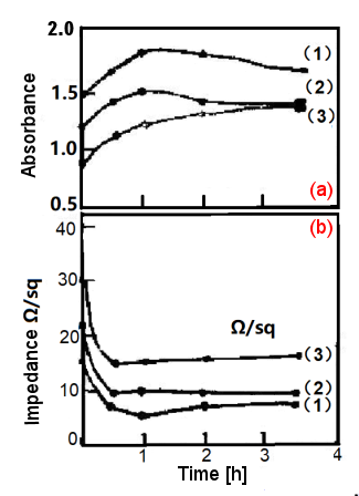
Fig. 2-5. The effect of annealing time on Pt film (glass substrate)
(a) Absorbance-time, (b) Impedance-time; annealing temperature 560 °C2-3)
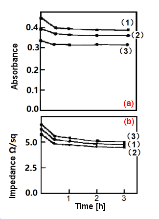
Fig. 2-6. The effect of annealing time on Au film (PbO2 on glass substrate).
(a) Absorbance-time, (b) Impedance-time; annealing temperature 200 °C2-4)
The resistance of these films can be reduced by about 10% to 30% by annealing in a muffle furnace. This artificial aging process may cause the discontinuous metal islands on the surface of the substrate to condense into a more continuous metal film, which reduces the resistance and improves mechanical adhesion and light transmittance, especially in the case of gold films. Fig. 2-5. shows the effect of annealing time on Pt film (glass substrate). It can be seen that the impedance decreases sharply at the beginning and reaches a normal value after 1 hour. In most cases, the impedance decreases by about 55% to 66%, and the permeability of the film lightness, gradually decreases with the annealing time. For the Au films on bismuth or lead oxide and ground in Fig. 2-6., the impedance and absorbance both decrease with annealing time.
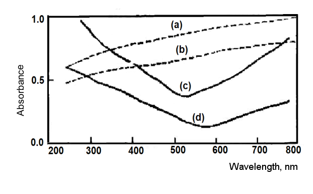
Fig. 2-7. Absorption spectra of various films on quartz substrate.)
Fig. 2-7. shows the absorption spectra of various films. The absorbance of Pt film is approximately linear in the wavelength range of 250 to 800 nm, while the absorption spectrum of gold film has a minimum at a wavelength of about 550 to 650 nm. When these metal films are deposited on a quartz substrate, the optically transparent electrode can be used for research in the ultraviolet region. Except that the overpotential of hydrogen ion discharge on the Pt thin film electrode is slightly lower than that of the bulk Pt electrode, the electrochemical properties of the gold thin film electrode are very similar to the bulk electrode.
Click to watch this lecture
References:
2-1) T. Kuwana and N. Winograd in Electroanalytical Chemistry, A. J.Bard. Ed., vol. 7, Marcel Dekker, New York, 1974.
2-2) N.R. Armstrong, A.W.C. Lin, M. Fujihira and T. Kuwana, Anal. Chem., 48, 741 (1976).
2-3) R. Cielinski and N. R. Armstrong, Anal, Chem., 51, 565 (1979)
2-4) W. von Benken and T. Kuwana, Anal. Chem., 42, 1114 (1970).

