Part 2: Manufacturing of IDA electrode
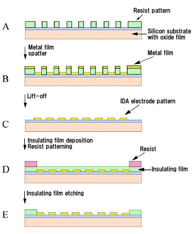
Fig. 2-1 shows a schematic of the manufacturing process of IDA electrodes.
A 3-inch silicon wafer substrate with oxide film is used. First, photoresist layer is coated on the substrate, and covered with a masking film with a pattern, followed by UV light exposure, and then developed with an alkaline solution to form an interdigitated array electrode pattern (A). Next, the substrate is placed in a sputtering device, and a thin layer (B) of metallic chromium coating and metallic gold is deposited in sequence.
In addition, the photoresist layer is dissolved in an organic solvent, and the unwanted metal covered by the photoresist is peeled off (lift-off) to obtain an interdigitated array electrode pattern (C). The entire surface of the pattern is covered with an insulating film, and the photoresist pattern is formed again on the areas that needs to be covered by the insulating film, such as the lead part (D), and the insulating film that is not covered with resist is dry etched until the electrode area is exposed (E).
On the other hand, using a process in which the entire substrate surface is first covered with a thin film of electrode material and then processed by an etching method, materials that are difficult to fabricate at low temperatures, such as carbon thin film with a wide potential window on the reduction side and ITO (transparent electrode), can be easily processed into microelectrodes [11].

Fig. 2-1 Schematic of manufacturing process of micro interdigitated array electrodes.
(☆ Some interdigitated array electrodes sold may vary slightly due to improvements, etc.)

